
10 Gbps Physical Layer for Single Twisted Pair
High data rates in vehicle networks could be achieved through multiple technical approaches. On the one hand this goal could be achieved by investing effort in the channel/transmission medium (see [1]). However, there is always the conflict between electrical requirements, like transfer function and electro-magnetic radiance/ susceptibility, and mechanical requirements, like weight, diameter, stiffness and used materials. The mechanical requirements indirectly stand for usability and costs of the cables. On the other hand, the goal of a higher data rate through the same channel can be achieved by investing in the signal processing at the end points. The development effort takes place up front and the only material costs are increased silicon area. Operating costs will rise by only the (unavoidable) power consumption in the network node; however, the goal of a new physical layer will be not to raise the power consumption per transmitted bit/s. The second option is the main focus of the presented work and technology.
The challenge
Major use cases for high-speed data transmission in vehicles are low-latency uncompressed video transmission and a network backbone of consolidated connections and busses. For the next generation of networks, data rates in the range of 10 Gbps – even up to the 12.5 Gbps required for high-resolution video distribution – are targeted. As a reference, application-proven lightweight cables like the star-quad are taken as a possible candidate for the transmission medium. Achievable lengths should be 10-15 m. At the targeted speeds, the transfer function of common cables becomes more problematic. Higher attenuation at higher frequencies surpasses practically compensable insertion loss in almost every cable type. Moreover, in certain cable types there is a notch present in the signal band in the frequency range from 2 GHz to 3,5 GHz. [2]
Furthermore, standard complementary metal oxide semiconductor (CMOS) technology itself becomes more bandwidth limiting at the target speeds. The parasitic transistor capacitances and a limited maximum transit frequency, and the ESD (electro-static discharge) protection at the pads, have a major influence on the transfer function of the channel. Additionally, the targeted speed conflicts with transmit power requirements for the cable lengths common e.g. in automotive applications. It is therefore the specific goal to increase throughput by adding intelligence on the semiconductor side and keeping the transmission medium light and low-cost. The core requirements selected for the development of the new physical layer were chosen to be a low deterministic latency, low power consumption, and the use of a single twisted pair. The target bit error rate was fixed at 10-12. The implementation had to be feasible on a standard CMOS process.
System overview
To tackle the design problem at hand, it was necessary to undertake a paradigm shift and abandon classical NRZ (non-return-to-zero) binary coding with relatively slim signal processing. Firstly, we moved to a higher level modulation format and thereby limited the transmission bandwidth, which is now well below the notch of conventional twisted pair cables. The choice for the modulation format was also made through the calculation of the so-called channel capacity of the chosen cable. (The channel capacity gives a theoretical maximum of achievable data rates; practical implementations are well below that number.) This calculation showed that binary coding at available transmit powers could not carry a 10 GBps data rate. It also showed which modulation complexity would yield optimal data rate performance on the channel. Secondly, the signal processing was moved into the digital domain to acquire more complex and powerful signal processing algorithms.
More specifically, a PAM4 modulation format was chosen. To facilitate the signal processing in the digital domain, a high-speed Digital-Analog-Converter (DAC) and an Analog-Digital-Converter (ADC) were implemented. The cable transfer function (low pass characteristic) is now compensated by two digital filters at transmitter and receiver working in tandem. These filters are adapted at run-time. The bit error rate is achieved and secured by adding error correcting redundancy encoding and decoding to the transmission system (so-called forward error correction).
CMOS implementation
Fraunhofer IIS has developed a hybrid prototype of an ASIC (application specific integrated circuit) and an FPGA (field-programmable gate array) to implement all these features of the new physical layer. The analog frontends (DAC and ADC) were implemented in the ASIC. This allows evaluation of the real circuit performance with all parasitic effects and getting reliable estimates for the overall power consumption, once analog and digital functionality is integrated together on a single chip. Moreover, with this implementation, the highest risk in system development was already addressed and the feasibility of the complete system could be shown.
The digital signal processing chain has been implemented in the FPGA. This gives flexibility in implementation details and parameterization of the different signal processing blocks. The implementation can also be tailored to the specific circuit performance of the analog frontends. After testing, debugging and optimization of features like self-adaptation, frequency synchronization and the link-start-up-procedure, the final tested version of the digital part can then be migrated to the ASIC. During the development, the performance of virtually all implementations of the converters and signal processing blocks was pushed, and match the state-of-the-art in their respective fields.

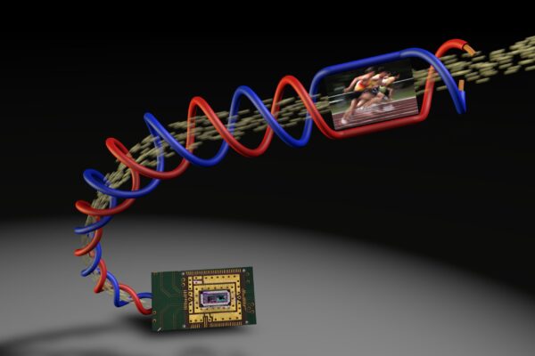
A picture of the prototyping platform can be seen in figure 1. It shows a flexible FPGA board (by the company “prodesign”), which can accommodate custom extension boards, one of which is hosting the ASIC with the analog frontends. From the performance of the analog chip and the complexity of the digital circuitry in combination with the required clock frequency, the overall power consumption of the targeted integrated system can be estimated. As a result, a transmitter and receiver pair will consume less than 1 Watt power on a 65 nm CMOS process. The latency of raw data through the link is below 10 µs even in the FPGA-based implementation. A picture of the implemented ASIC can be seen in figure 2. Data transmission experiments have begun recently. Although the engineering team is currently at about 80% of targeted throughput, testing and parameterization is ongoing and they are confident about pushing the envelope on this figure in the near future.

© Fraunhofer IIS
Conclusion
Fraunhofer’s development of the physical layer is a core technology for future data transmission links and networks based on short- to medium-range twisted-pair cables or comparable media. It answers the questions of how to get raw data over the copper cable, how to start up the link and facilitate the full-speed transmission, and how to manage physical link health during operation. During the course of the physical layer development, the copper cable itself was also investigated. They found it to be a design item within the physical layer that can be tailored to the application at hand. Through a systematic process, they managed to reduce insertion loss while at the same time reducing weight (see [1] for details).
For example, one could also use the more advanced signal processing of the presented technology and “reduce on the cable side” to decrease weight and/or material usage there. Fraunhofer IIS, with a paradigm shift in the signal processing scheme and a big development step of a hybrid prototype, has opened the door to the next generation of high-speed data transmission. It paves the way to faster, lighter and more efficient data links and networks in automotive applications.
[1] C. Zerna et. al., „Computer-Aided Optimization of Copper Cables for High-Speed Data Transmission”, ITG-Fachtagung Kabelkommunikationsnetze, Köln 2014
[2] R. Kraus, “APIX auf der Überholspur”, Elektronik, 1.6.2010
Authors:
Norbert Weber, Ph.D: is head of the project group optical sensors and communications at the Fraunhofer Institute for Integrated Circuits, Germany since 1999. Currently his research interests include high-speed circuit design and optical communications.
Conrad Zerna: is working in the project group optical sensors and communications at the Fraunhofer Institute for Integrated Circuits, Germany since 2008. He has developed several equalizers of different architectures for data transmission speeds ranging from Mbit/s up to 10 Gbit/s and is currently executive project leader for the new physical layer development.
 If you enjoyed this article, you will like the following ones: don't miss them by subscribing to :