
Renesas meets automotive image processing challenges
The image processing circuitry for autonomous vehicles is required to integrate the functionality of both in-vehicle infotainment systems and driving safety support systems, and to operate both in parallel. In particular, driving safety support systems must be able to process video data from vehicle cameras with low latency to notify the driver of appropriate information in a timely manner. One issue that developers of in-vehicle infotainment systems and driving safety support systems face is the need to process large amounts of video data and also to perform autonomous vehicle control functions, without delays and instability.
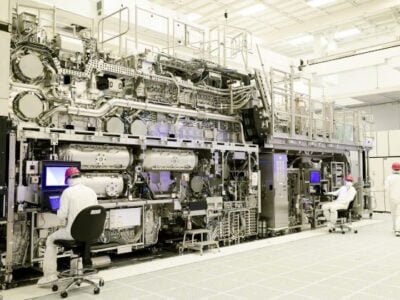
Renesas’ new video processing circuit block handles processing of vehicle camera video with low latency. It can perform video processing in real time on large volumes of video data with low power consumption and without imposing any additional load on the CPU and graphics processing unit (GPU), which are responsible for autonomous vehicle control. Renesas has manufactured prototypes of the new video processing circuit block using a 16 nanometer (nm) FinFET process. In addition to 70ms-latency processing of vehicle camera video, it delivers industry-leading Full-HD 12-channel video processing with only 197 mW power consumption.
Recently, in-vehicle infotainment systems foreshadowing the future emergence of autonomous vehicles, such as car navigation systems and advanced driver assistance systems (ADAS), have made significant advances that bring them closer to becoming automotive computing systems integrating the functionality of both in-vehicle infotainment systems and driving safety support systems.
The video processing circuit block can decode video streams transferred from vehicle cameras and apply distortion correction, with low latency. It performs the complex video processing required by automotive computing systems, delivering real-time performance and low power consumption, while imposing no additional load on the CPU and GPU responsible for cognitive processing tasks.
Key features of the technology:
- Synchronous operation among video processors, combined with pipeline operation, for video decoding and distortion correction with 70ms latency
- 17 video processors of six different types, optimized for automotive computing systems to deliver industry-leading Full-HD 12-channel performance
- Combination of two types of data compression, lossless compression and lossy compression, to reduce memory bandwidth by 50 percent and achieve Full-HD 12-channel processing with industry-leading low power consumption of 197 mW.
Renesas announced this technology on February 1 at the International Solid-State Circuits Conference (ISSCC) held in San Francisco from January 31 to February 4, 2016. The demonstration showed the processing performance of a test board with an SoC incorporating the newly developed video processing circuit block by playback of Full-HD 12-channel video content, accompanied by a real-time display of memory bandwidth reduction rate.
The circuit block shown currently represents a collection of IP, demonstrating methods to optimise the tasks of video processing at the semiconductor level, a Renesas spokesperson commented. It is not available at the maket yet, but it can be expected that it will be encountered in possible slightly modified form in some of the company’s next-generation products.
 If you enjoyed this article, you will like the following ones: don't miss them by subscribing to :