Power MOSFET Basics: Understanding the superjunction technology
Power MOSFETs based on superjunction technology have become the industry norm in high-voltage switching converters. They offer lower RDS(on) simultaneously with reduced gate and output charges, which allows for more efficient switching at any given frequency.
Prior to the availability of superjunction MOSFETs the dominant design platform for
high-voltage devices was based on planar technology. However, fast switching at high
voltages poses its own challenges in AC/DC power supplies and inverters. Designers
making the transition from planar to superjunction MOSFETs often have to accommodate EMI, voltage spikes, and noise-related concerns by compromising switching speed. Below we will compare the characteristics of the two platforms so that the benefits of superjunction technology are fully understood and utilized.
In order to understand the differences between the two technologies, we need to start
with the basics. Figure 1a shows the simple structure of a conventional planar high-
voltage MOSFET. Planar MOSFETs typically have a high drain-to-source resistance per unit of silicon area, and come with relatively higher drain source resistances. Lower RDS(on) values could be achieved with high cell density and large die sizes. However, large cell densities and die sizes also come with high gate and output charges, which increase the switching losses as well as costs. There is also a limit to how low the total silicon resistance can go. The total RDS(on) for the device can be expressed as the sum of three components: the channel, epi, and the substrate.
RDS(on) = Rch + Repi + Rsub

Figure 1a: Conventional Planar MOSFET Structure

Figure 1b: Resistive Components of a Planar MOSFET
Figure 1b shows a breakdown of different components that make up the RDS(on) in a
planar MOSFET. For low-voltage MOSFETs the three components are comparable. However, as the voltage rating is increased, the epitaxial layer needs to be thicker and more lightly doped to block high voltages. For every doubling of the voltage rating, the area required to maintain the same RDS(on) increases more than five-fold. For 600 V rated MOSFETs, more than 95 % of the resistance comes from the epitaxial layer. It is obvious that for any significant reduction in the RDS(on) value, it is necessary to find a way of heavily doping the drift region and drastically reducing the epi resistance.

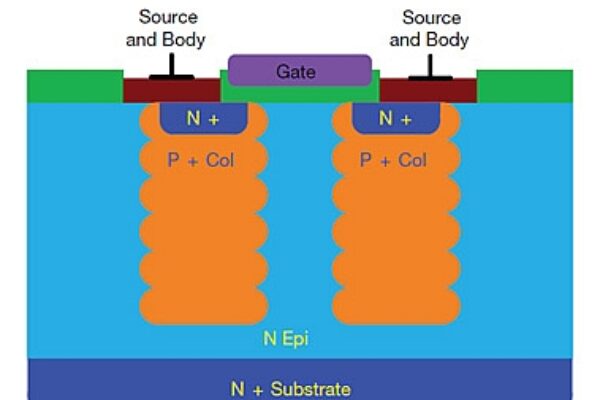
Figure 2: Superjunction MOSFET Structure

Figure 3: Blocking Voltage and On-resistance Comparison for Planar and Superjunction
MOSFETs
Figure 2 shows the physical structure of superjunction MOSFETs based on the idea of charge balancing. The drift region now has multiple P columns, which cancel the charge in the surrounding N regions under reverse bias. As a result, the Nepi can now be thinner and heavily doped since the combined structure offers a much higher resistance to applied reverse voltage. As the N region becomes more heavily doped, its on-resistance per unit area decreases.
Figure 3 compares the electric field in the drift region vs. epi thickness for the two
technologies. In conventional planar MOSFETs, the blocking voltage is defined both by the epi thickness and the doping (ND+), or slope of the line. If additional blocking
voltage is required, not only does the epi have to be made thicker, but the epi doping
line also has to change. This results in a disproportionate increase in RDS(on) for
higher-voltage MOSFETs. For every doubling of voltage rating, keeping the same die
size, the RDS(on) can increase anywhere from three- to five-fold.
Superjunction MOSFETs can use a thinner epi (A1 + A2) for a given blocking voltage than conventional planar devices (A1 + A3). The doping of the N region (ND+) is balanced out by the doping of the P column (NA-), resulting in no slope. In other words, because of the charge balancing mechanism, only the thickness of the epi defines the blocking voltage. As a result, the superjunction structure has a linear relationship between on-resistance and breakdown voltage. The on-resistance increases linearly with an increase in breakdown voltage. For the same breakdown voltage and die size, the on-resistance of a superjunction MOSFET will be much less than a conventional planar device.
CAPACITANCES
The reduction in resistance for superjunction devices has obvious benefits, such as lower conduction losses or smaller dies for the same RDS(on). Additionally, the reduction in the chip area can lead to lower capacitances and gate and output charges, which reduces dynamic losses. In low-voltage trench or planar MOSFETs, there is usually a trade-off between lowering the RDS(on) at the cost of higher capacitances. In the case of superjunction technology the compromise is minimal. The charge balancing mechanism achieves simultaneous reduction in RDS(on) and device capacitances, making it a win-win solution.

Table 1 compares the characteristics of two devices with close RDS(on) values. The superjunction device has 15% to 25% improvement for every parameter, except for Eas and Ias. This is because the superjunction device, despite a 20% reduction in RDS(on), has a die size that is only one third of the comparable planar. The smaller size affects current and power ratings. A large die size has lower current density and better heat sinking capabilities. As a result, for a given on-resistance, the conventional planar MOSFETs are inherently more rugged compared to superjunction devices. However, at currents and switching frequencies typically used in high-voltage power converters, the superjunction device will always offer lower loss and better efficiency.

Table 2 shows another comparison, this time for 500 V devices. The planar MOSFET has a 125 mΩ typical RDS(on) rating. The die is large, in fact the largest die that can fit into a TO-247 package. This can be compared with a superjunction device in the smaller, isolated thin lead TO-220F package, which offers the same RDS(on) but better specifications on every parameter except UIS ruggedness. It should be noted that Vishay is quite conservative in derating the inductive switching specifications. A 100% derating factor is applied on the measured failure current, which translates to a derating factor of four for UIS energy Eas.
Figure 4 defines the capacitances for which the charge specifications are provided. For the two 600 V devices compared above, the capacitance curves are shown in Figure 5. Note that the capacitance scale is logarithmic.

Figure 4 : MOSFET Capacitance Definitions

Figure 5: Capacitance Comparison for Planar and Superjunction MOSFETs
Gate Charge Considerations
In any switching circuit the gate drive design is a trade-off between switching speed and noise. Superjunction devices offer high switching speeds at high voltages, which also demand extra attention to drive design. Poor design may cause voltage spikes, erratic switching, and higher EMI. Another major concern with ultra-low capacitances is an increased sensitivity to coupling and noise, which shows up as gate source oscillation. Designers are then forced to slow down the switching speed by introducing high gate resistances or low drive currents, which ultimately reduce the system efficiency.
The mechanics of power MOSFET turn on and off behavior has been studied in detail, [1], [2]. In high voltage applications the rise and fall times of MOSFET Vds require special attention. Typically, the Qgd of a MOSFET can be used for estimating the VDS voltage rise and fall times during switching. Assuming a constant current source driving the gate, tvfall = Qgd / Igon and tvrise = Qgd / Igoff. This simple model cannot be used for superjunction devices, whose structure and switching behaviors are more complex.
As an example, Figure 6 shows the gate charge curve for a superjunction device with a VDS curve superposed on it. One feature of superjunction MOSFETs when compared to planar devices is the wide variations in their capacitances as a function of VDS. In a superjunction MOSFET, because of the 100:1 drop in Crss from 0 V to 600 V, the observed switching durations will appear to be much smaller than those estimated from the datasheet values of Qgd.
While there is no analytical method to predict the actual transition times, which in turn depend on application conditions, designers should be aware that good switching performance can be achieved with lower gate drive currents. This translates into smaller and lower-cost gate drivers compared to those used for planar MOSFETs.

Figure 6: Gate Charge vs. VDS for a superjunction MOSFET.

Figure 7: Capacitance and Stored Energy vs. VDS for a superjunction MOSFET.
Coss, Co(tr), Co(er), and Eoss
Figure 5 also shows that Coss for the superjunction device is nearly 40% lower, leading to reduced stored energy and faster switching, while at the same time achieving lower loss. The output capacitance Coss of all MOSFETs shows non-linear characteristics with respect to applied voltage VDS. The non-linearity is even more pronounced in the case of superjunction MOSFETs, with a variation of 100:1 in value from 0 V to 600 V. This poses a challenge to designers who need effective values for stored charge and energy in the Coss. The superjunction datasheets typically provide two effective values for Coss, defined as follows:
Co(tr) – defines the value of a fixed capacitor, which has the same stored charge as the variable Coss at 80% of the rated voltage.
Co(er) – defines the value of a fixed capacitor, which has the same stored energy as the variable Coss at 80% of the rated voltage.
Several studies have emphasized the impact of stored energy Eoss on system efficiency under different operating conditions. Recognizing the importance, Vishay has started providing complete Eoss curves for high-voltage superjunction MOSFETs, all the way up to rated voltage as shown in Figure 7.
Body Diode Characteristics
Because of their combination of lower RDS(on) and low capacitances, superjunction MOSFETs are also the devices of choice for all high-frequency switching applications, including ZVS bridges. In a ZVS or synchronous application, the body diode of the MOSFET is not subject to hard commutation. The diode current is softly commutated to the MOSFET channel and the diode recovers voltage blocking capability when the MOSFET is turned off. However, this does not mean that diode recovery can be taken for granted in ZVS bridges under all operating conditions, including transients.
Lower Qrr, short carrier lifetime, and soft recovery characteristics are still important requirements. Superjunction MOSFETs do have the advantage of lower Qrr and trr over planar devices and therefore are better suited in ZVS applications. However, where the ability of the body diode to recover blocking voltage is considered critical, further improvements in the recovery characteristics are desirable. Recognizing the need, Vishay has introduced the EF series of superjunction MOSFETs in which, using additional processes during manufacturing, the Qrr of the body diode is reduced by a factor of 5 to 7.
Conclusions
The superjunction structure is a major development in high-voltage MOSFET technology and offers significant benefits. RDS(on), gate capacitances, and output charge are all simultaneously reduced, along with die size. To make the best use of these fast and efficient devices, designers have to pay greater attention to their system design, particularly towards reducing PCB parasitics. Superjunction MOSFETs have much lower gate charges and can be driven with low-current gate drivers. Their output capacitances, while highly non-linear, offer lower stored energy Eoss and related output losses. A wide variety of superjunction devices are available today in different packages, voltage ratings, and body diode characteristics to suit a variety of applications.
[1] Vishay Application Note AN-608,”Power MOSFET Basics: Understanding Gate Charge and Using it to Assess Switching Performance,"
[2] Vishay Application Note AN-850: “Power MOSFET Basics: Understanding the Turn ON Process”
 If you enjoyed this article, you will like the following ones: don't miss them by subscribing to :