Stepping into next generation ADAS multi-camera architectures
Introduction
Multi camera systems are common for the development of Surround View and Mirror Replacement Applications. Today’s systems can have six cameras or more to observe and identify the scene around the car. In surround view, typically a minimum of four camera streams will be stitched together for the best driver experience. This architecture normally interconnects megapixel image sensors with one central applications processor by bridging the long distance over single coax cables. In addition, the market demands pixel precision at a higher dynamic range to further optimize vision algorithms. This requires an additional step of pixel post processing.
Therefore, next generation systems feature central clock distribution, video line synchronization and multi-channel pixel processing providing much better video quality to the driver. In particular, the coaxial cable’s back channel capability plays a significant role. In order to achieve all this chip-sets of multiple LVDS serializers combined with a single deserializer hub feature highly integrated solutions. This paper discusses how video stream synchronization can be achieved and how pixel precision can be increased.
Image Sensor Technology
Today’s CMOS color imagers provide 1-megapixel or 2-megapixel on a single-chip for automotive applications. They record highly detailed full-resolution images, providing video streams up to 60 frames per second (fps). The sensors may use split pixel HDR technologies, in which the scene information is sampled simultaneously rather than sequentially. It minimizes motion artifacts and delivers superior image quality in RAW output in demanding and difficult lighting conditions. In order to extend pixel precision to up to 12 bits of dynamic range, the sensor reads out up to three exposure values per pixel, “long (L)”, “short (S)” and “very short (VS)”. These are used to further process high dynamic range images when fed into an image signal processor (ISP). Currently, image sensor manufacturers are moving the ISP function out of the imager chip in order to limit power dissipation impacting the quality of the image. Hence, ISPs will be integrated into the vision processors (SoC) or remain as standalone devices. With advanced HDR capabilities, ISPs can even process multiple camera streams concurrently, limiting the number of ISP devices in the system. In particular, centralized processing of such a kind can benefit from multiple-stream processing during equalization steps. To accomplish this, camera streams need additional indication for channel separation. Otherwise, the video streams may get mixed up in the system path.
Multi-Channel Pixel Processing
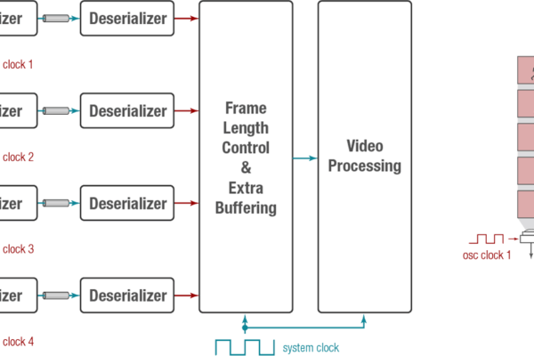
This section discusses the signal chain of the TI reference design “TIDA-00455” (See Figure 1). FPD-Link III serializers as such as the DS90UB933 transform an incoming parallel LVCMOS or a serial CSI-2 data bus into a single high-speed differential pair. The serializers can accept up to 12-bits of data + 2 bits (e.g. HSYNC/VSYNC) + pixel clock (PCLK). In turn, the FPD-Link III deserializer hub (e.g. DS90UB964) when coupled with serializers receives the streams from up to four image sensors concurrently. It provides two MIPI CSI-2 output ports consisting of four physical lanes each. The deserializer decodes incoming streams to be multiplexed on one or two of the MIPI CSI-2 output ports. In order to keep incoming video streams separated, the MIPI CSI-2 ports offer up to four virtual channels. Every data stream is partitioned into packets designated for each virtual channel. A unique channel identification number (VC-ID) in the packet header identifies the virtual channel. Virtually separated the video streams will be sent out through the CSI-2 ports. The image pixels of the video streams arrive at the ISP, separated in long (L), short (S) and very short (VS) exposure values indicated by its MSB each. When multiple pre-processing steps as such as lens correction, white balancing or defective pixel correction are completed, the ISP combines the values with different exposures to generate image frames. Dark areas will be filled with pixels from L exposure values while bright areas will be filled with pixels from either S or VS values. As a result, the image pixels of each video stream provide extended dynamic range. The weighted output of the combination feeds back into the blocks as such as automatic gain control (AGC), automatic exposure control (AEC) in order to calculate statistics. The statistics including histogram can be transferred to the host as part of idle rows within the video stream. Finally, high quality video streams will be transmitted into the vision processor for image rendering and vision analytics purposes prior to be displayed on a monitor.

Achieving Video Stream Synchronization
For these system designs, camera synchronization can become a challenge. Processing time of each camera can vary due to component tolerances or even conditions in the visual scene being recorded. Time stamp mechanisms would need to be introduced in software to overcome the problem. However, additional software would further utilize the vision processor. As a solution four hardware features are discussed as follows ensuring frames from all video streams arrive in the vision processor at same time. No additional software engagement would be required.
Back Channel Technology
The SerDes integrated bidirectional control channel transfers data over the same cable. It eliminates the need for additional wires for programming the image sensors’ registers via I2C. The bidirectional control channel also allows controlling GPIO pins of the SerDes chips in both directions. Commonly, this is used to send frame sync trigger pulses from the central processing unit into the image sensors for synchronization. Concurrently, it can carry status signals from all image sensors and pass it on to the central processing unit for monitoring purposes. The bidirectional control channel can also carry a central system reference clock from the deserializer to each camera serializer.

Central Clock Distribution
A central reference clock applied at the deserializer hub is distributed to all camera modules. In this mode, each serializer is able to derive its clock from the FPD-Link III system link. The serializers drive the clock into the image sensor’s system clock input pin avoiding the camera streams to drift past each other. Operation in this mode offers the advantage that all the cameras can operate in the same clock domain. It eliminates the need for data buffering and re-synchronization.


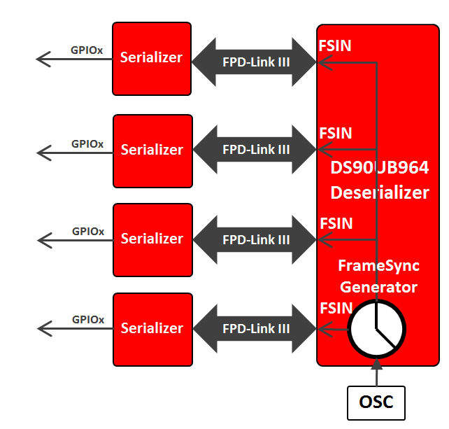
Central Frame Synchronized Trigger
Common image sensors offer one frame synchronization input (see FSIN in the block diagram). FSIN controls the image sensor’s capture logic. During normal operation, when the frame synchronization pulse is applied, a new frame will start automatically. Alternatively, one additional line will be introduced to extend the frame height until frame synchronization arrives. An appropriate deserializer hub can generate such a periodic synchronization pulse using its internal timer. The deserializer hub passes the periodic frame sync pulse to all the serializers. In turn, the serializers pass the pulse to each camera using its GPIOs. This concept guarantees frames from all camera streams start simultaneously with a variance of one line maximum.
Line based Synchronization
Commonly, deserializer hubs support several line synchronization modes. In Non-Synchronized Forwarding Mode, the deserializer hub embeds the lines from all video streams in a first come, first send order. The same video lines from all cameras do not arrive in the ISP at the same time. Hence, lines captured at the same time are not stored in the buffer queues of the vision processor sequentially. In Synchronized Forwarding Mode however, the deserializer hub waits for the video lines from all camera modules to arrive prior to encoding the lines and embedding them into the CSI-2 output stream. As a result, the same lines from all cameras are interleaved. Deserializer’s job is to pack the incoming streams into one or two MIPI CSI-2 output streams. To do so, the use of virtual channels (VC-ID) are used to differentiate video streams on the MIPI CSI-2 output bus. Hence, the ISP and further the vision processor are able to distinguish the streams. If the vision processor is programmed to provide four independent buffer queues in memory, frames from each of the video streams can be stored in their own queue. This method leads to a scheme in which each frame captured at same time will be stored in the queues side by side. For instance, the frame from all the four streams captured at time slot x can be found in buffer queues at the same location x. Therefore, no timestamp support is required.

Power-over-Coax (PoC)
Applying power over the data coax cable, or power-over-coax (PoC), provides a convenient way to power the camera without extra cabling. In order to save additional wires, the camera modules can be supplied over the coax line and the shield from the processor ECU side. On the deserializer side power can be injected to supply all camera modules. In order to separate the DC power supply from the data signals, PoC filters need to be incorporated. The data signal frequency band begins at 1MHz for the back channel (depending on serializer backchannel speed). In contrast, the forward channel band can go higher than 700MHz. Hence, a 100nF capacitor needs to block any DC to pass. On the other side one 100uH inductor passes the DC but helps minimize AC noise interfering with the data signals.
Carefully laying out and tuning both the components will ensure power to transmit over the coax cable but avoid impacting the AC signal. Please see the following Application Report for more details on PoC filter design: www.ti.com/lit/an/snla224/snla224.pdf.

Vision Processing
The TDA2x Vision Processor, illustrated in Figure 1 requires the ISPs to remain external. However, the TDA3x Vision Processor incorporates the ISP on-chip. Hence, higher level of integration can be achieved. Due to its video port (VIP) capability the video streams arrive in the processor’s memory without burdening the processing cores. Instead, the VIP’s DMA controller ensures all video streams to be stored in its frame buffers. In turn, the processing cores receive notifications on interrupt level when new frames arrive. The processor’s software accesses the frame buffers as needed to process the video data.
Conclusion
Self-driving cars will demand a high number of sensor technologies in order to completely map its environment. Sensor technologies as such as Vision, Radar and LIDAR will play a significant role. Sensors will be mounted around the car and therefore need compact, low-cost cabling to connect satellite sensors to a central fusion processing unit. FPD-Link III solutions fulfill those demands future sensor fusion systems.
For more information please visit: https://www.ti.com/product/ds90ub964-q1 and https://processors.wiki.ti.com/index.php/TIDA-00455_-_Automotive_ADAS_4_Camera_Hub_with_integrated_ISP_and_DVP_outputs
About the author:
Thorsten Lorenzen is Senior Field Application Engineer for automotive ADAS applications at Texas Instruments. He studied electrical engineering and electronics engineering at the THM in Giessen/Germany and at the University of Central Lancashire in Preston/UK.
 If you enjoyed this article, you will like the following ones: don't miss them by subscribing to :